
All Products
Contact Person :
Anna
Phone Number :
18620306819
WhatsApp :
+18620306819
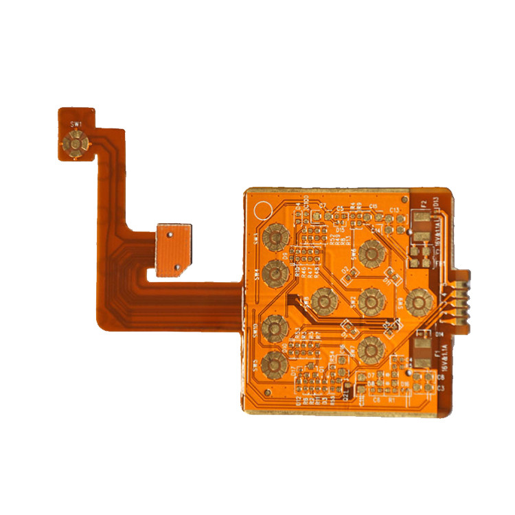
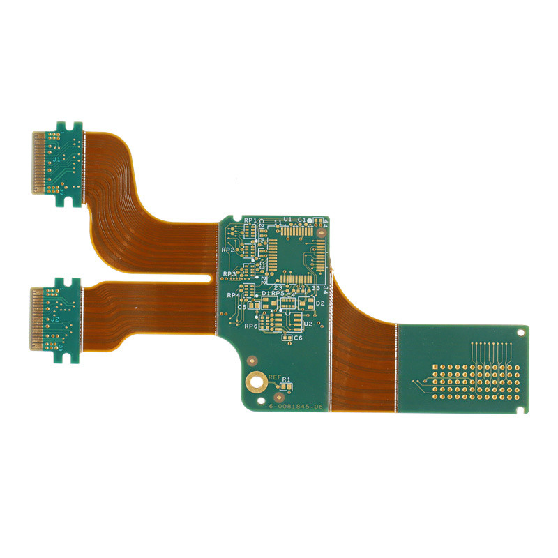
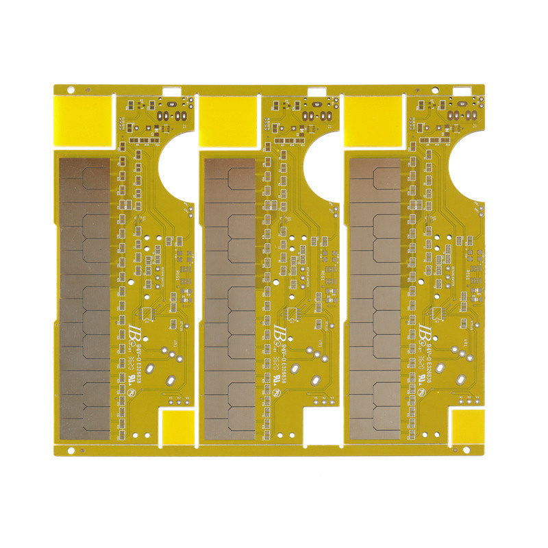
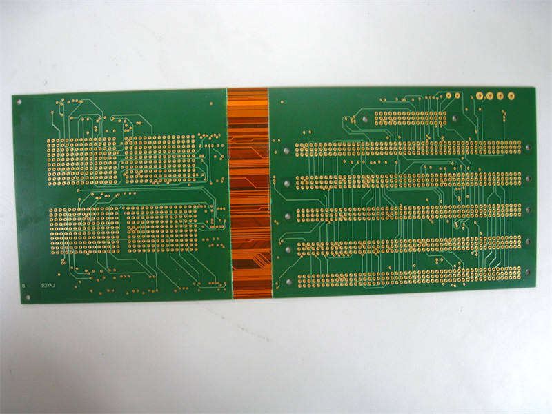
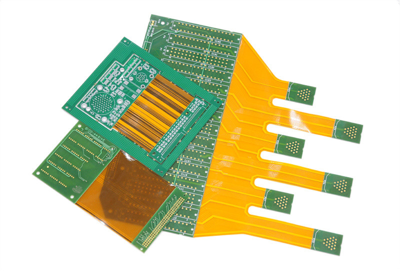
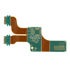
Blind And Buried Via HDI Rigid Flex Pcb Multilayer ATF 16949


| Place of Origin | China |
|---|---|
| Brand Name | IBE |
| Certification | ISO/TS16949 ISO13485 |
| Model Number | Flexible PCB |
| Minimum Order Quantity | 10 |
| Price | $0.1-$0.5 |
| Packaging Details | ESD bag |
| Delivery Time | 5-8 working days |
| Payment Terms | D/A, L/C, D/A, D/P, T/T, Western Union, MoneyGram |
| Supply Ability | 50000pcs/week |
Product Details
| Min. Line Width | 0.075mm/0.075mm(3mil/3mil) | Surface Finishing | ENIG |
|---|---|---|---|
| Copper Thickness | 1oz | Base Material | FR4 |
| Min. Line Spacing | 0.075mm | Board Thickness | 1.6mm |
| Min. Hole Size | 0.25mm | Soldermask Color | Blue |
| Silkscreen Color | White | Layer | 1-32L |
| High Light | Blind And Buried Via Multilayer Pcb,ATF 16949 hdi rigid flex pcb,ATF 16949 Multilayer Pcb |
||
Product Description
Our Advantages:
1, Factory Area:60000㎡ Shenzhen factory; two other factories in US and Vietnam.
2, Quality Control:IPC-1-610E Standard,E-test,X-ray,AOI Test,IQC,QC,QA,100% Functional Test
3, PCB Making (Rigid, Flexible,Rigid-Flexible,Aluminium, High TG,Ceramic), Component Sourcing, SMT&DIP, Free Program & Test, OEM/ODM Serivce
4, Certifcation:ATF 16949,ISO 13485,ISO 14001,ISO9001,UL(E326838),Disney FAMA, CE,FCC,ROHS,
| 1 | Material | PR4,Halogen free, High TG,CEM3,PTFE,Aluminum BT,Rogers |
| 2 | Board Thickness | Mass Production:0.3-3.5mm Samples:0.21-6.0mm |
| 3 | Surface Finish | HASL,OSP,Immersion Silver/Gold/SN,Flash Gold, Gold Finger,Hard Gold Plating |
| 4 | PCB Panel Size | Max Mass Productoin: 610x460mm Sample:762x508mm |
| 5 | Layer | Mass production:2-58 Layers, Samples:1-64 Layers |
| 6 | Min. Drill Hole Size | Laser Drill 0.1mm,Machine Drill 0.2mm |
| 7 | PCBA QC | X-ray,AOI Test,Functional Test |
| 8 | Speciality | Automotive,Medical/Gaming/Smart Device,Computer,LED/Lighting,etc |
| 9 | Sanforized | Buried via, Blind via, Mixed Pressure,Embedded Resistance,Embedded Capacitance, Local Mixed Pressure, Local High Density, Back Drill, Impedance Control |
PCBA Capability
The main SMT production line consists of automated high-precision state-of-the-art equipments from PanasonIC,Sumsung, Japan total 6 lines (Smallest SMT components size can reach to 0201,capable of 0.6mm*0.3mm ~ 50mm*50mmQFP, 0.15mm gap, ±0.05 accuracy ),
EMS capacity can reach 150,000,000 components per month.
Our engineering team has extensive experience in DFM/DFA/DFT technologies.
SMT, BGA Rework, Re-balling, X-Ray are all readily achieveable. Stencils can
be cut and delivered inside of 4 hours.
| PCB Assembly Capability | |
| Stencil size range: | 1560*450mm |
| Min SMT package: | 0402/1005(1.0x0.5mm) |
| Min IC pitch: | 0.3mm |
| Max PCB Size: | 1200*400mm |
| Min PCB thickness: | 0.35mm |
| Min Chip Size: | 01005 |
| Max BGA Size: | 74*74mm |
| BGA Ball Pitch: | 1.00~3.00mm |
| BGA Ball Diameter: | 0.4~1.0mm |
| QFP Lead Pitch: | 0.38~2.54mm |
| Testing : | ICT,AOI,X-RAY,Funtional test etc. |
Delivery Time:
|
Order Conditions
|
Standard Delivery Date
|
The fastest Delivery Date
|
|
Prototype ( <20pcs)
|
2days
|
8hours
|
|
Small Volume (20-100pcs)
|
6days
|
12hours
|
|
Medium Volume (100-1000)
|
3days
|
24hours
|
|
Mass Production (>1000)
|
Depends on BOM
|
Depends on BOM
|
FAQ:
1. What’s a motherboard?
![]()
A motherboard is a printed circuit assembly(PCA) used exclusively in laptop or desktop computers. While some may refer to a PCA as a motherboard,only those found in computers are motherboards. All other printed circuit assemblies are simply PCA or PCBA.
2.How does a printed circuit board assembly (PCB assembly) work?
![]()
The primary function of a PCB assembly is to integrate the electronic components of a device into a compact or defined space. Acting as the central hub of the electronic circuit of a device, the PCB provides insulation for all other electrical components, allowing them to be safely connected to a power source.
3. What information is required for a turnkey PCB assembly order?
For turnkey projects, we’ll need the following:
Gerber file
Bill of materials (BOM)
Component placement list (CPL)
All relevant CAD and .stp file
4. Are you UL / Underwriters Laboratory approved?
IBE pursues all applicable UL certifications for our products, and we offer several products certified with UL and CSA based on customer’s demand
Underwriters Laboratories (UL) grants multiple certifications, including:
IBE is certified for PCB by UL file E326838
5. Do you offer RoHS&REACH-compliant assemblies?
Yes, IBE does offer assemblies that comply with the European Union’s Restriction of Hazardous Substances (RoHS) Directive and REACH.
6. Do you offer testing and inspection services?
Yes, IBE offers a comprehensive list of testing and inspection services for both SMT and through-hole assemblies.
Visual inspection/scanning microscopes
AOI inspection
In-circuit test
Functional testing include automated test equipment and system
Burn-in tests
Low/High Temp Chamber Testing
X-ray inspection and repair
Salt fog tester
Drop Test
packing vibration
Conformal coating and potting
7. What are your PCB assembly standards?
IBE has obtained the following IPC electronics industry standards for PCB assembly
IPC-A-600G for PCB production
IPC-620 for practices and requirements for cables, wire, and harness assembly manufacturing
IPC-A-610E PCBA Acceptability of Electronic Assemblies
8.Where do you manufacture your products?
We have production plant based in shenzhen,China; Fremont,US,Bac Ninh,Vietn
Recommended Products