


All Products
ENIG Immersion Gold Plating 2 Layers PCB IATF TS16949 ISO13485 ISO 9001


| Place of Origin | CHINA,VIETNAM,USA |
|---|---|
| Brand Name | IBE |
| Certification | UL |
| Model Number | FG-07 |
| Minimum Order Quantity | NO MOQ |
| Price | Negotiable |
| Packaging Details | BAG |
| Delivery Time | 15 WORKING DAYS |
| Payment Terms | L/C, T/T |
| Supply Ability | 100000pcs |

Contact me for free samples and coupons.
Whatsapp:0086 18588475571
Wechat: 0086 18588475571
Skype: sales10@aixton.com
If you have any concern, we provide 24-hour online help.
xProduct Details
| Colour | Green | Material | Halogen Free |
|---|---|---|---|
| Layer | 2 | Surface Technical | ENIG |
| Max Panel Size | 800mm*508mm | Name | PCB |
| Highlight | Immersion Gold Plating 2 Layers PCB,2 Layers PCB IATF TS16949,ENIG immersion gold PCB ISO13485 |
||
Product Description
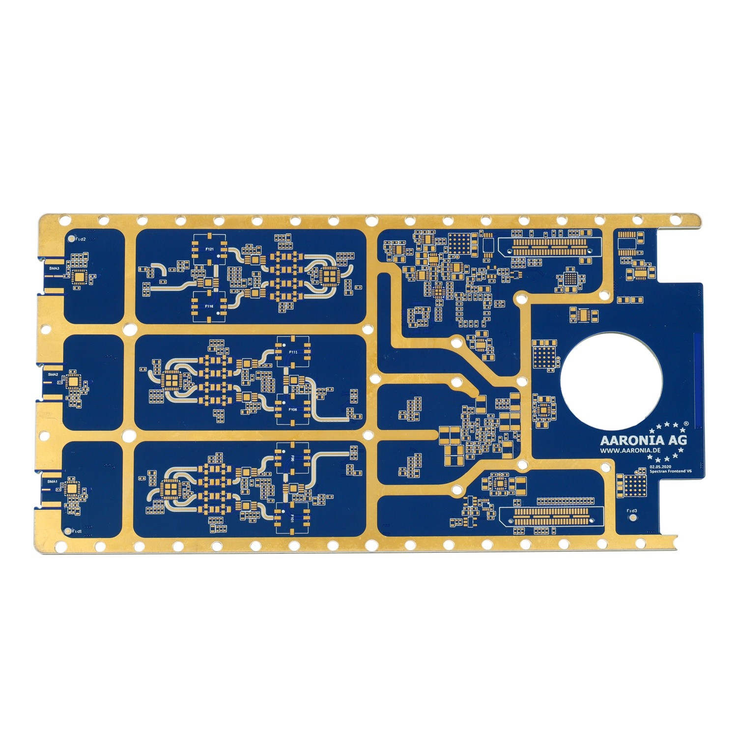
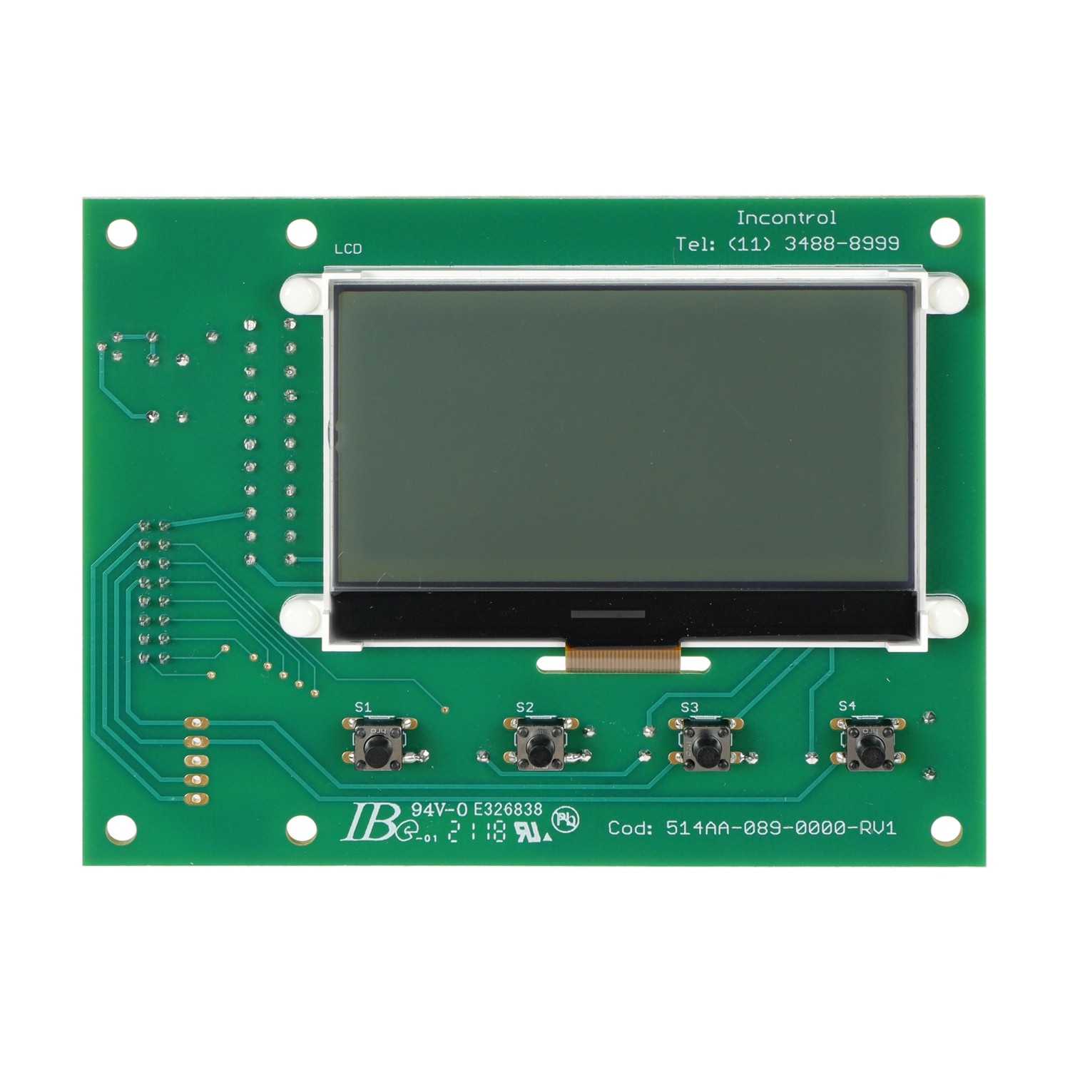
What is a 2 Layer PCB?
2 layer PCB ( double-sided PCB )is a printed circuit board with copper coated on both sides, top and bottom. There is an insulating layer in the middle, which is a commonly used printed circuit board. Both sides can be layout and soldered, which greatly reduces the difficulty of layout, so it is widely used.
Our Advantages:
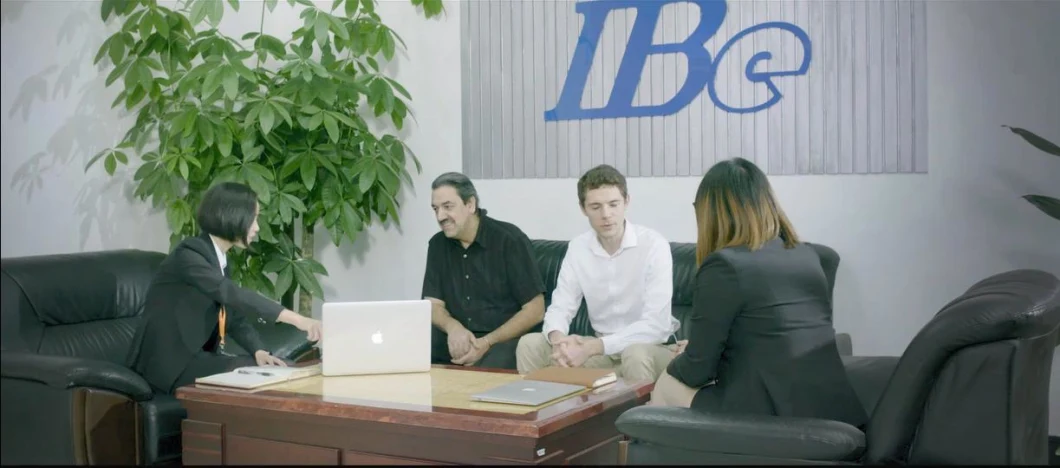
1, PCB Making (Rigid, Flexible,Rigid-Flexible,Aluminium, High TG,Ceramic), Component Sourcing, SMT&DIP, Free Program & Test, OEM/ODM Serivce
2, Factory Area:60000㎡ Shenzhen factory; two other factories in US and Vietnam
3, Certifcation:ATF 16949,ISO 13485,ISO 14001,ISO9001,UL(E326838),Disney FAMA, CE,FCC,ROHS,
4, Quality Control:IPC-1-610E Standard,E-test,X-ray,AOI Test,IQC,QC,QA,100% Functional Test
Production capability:
| 1 | Material | PR4,Halogen free, High TG,CEM3,PTFE,Aluminum BT,Rogers |
| 2 | Board Thickness | Mass Production:0.3-3.5mm Samples:0.21-6.0mm |
| 3 | Surface Finish | HASL,OSP,Immersion Silver/Gold/SN,Flash Gold, Gold Finger,Hard Gold Plating |
| 4 | PCB Panel Size | Max Mass Productoin: 610x460mm Sample:762x508mm |
| 5 | Layer | Mass production:2-58 Layers, Samples:1-64 Layers |
| 6 | Min. Drill Hole Size | Laser Drill 0.1mm,Machine Drill 0.2mm |
| 7 | PCBA QC | X-ray,AOI Test,Functional Test |
| 8 | Speciality | Automotive,Medical/Gaming/Smart Device,Computer,LED/Lighting,etc |
| 9 | Sanforized | Buried via, Blind via, Mixed Pressure,Embedded Resistance,Embedded Capacitance, Local Mixed Pressure, Local High Density, Back Drill, Impedance Control |
FAQ:
Q: What service do you have?
A: We provide PCBA turnkey solution including PCB fabrication, SMT, wire harness assembly & sheet metal fabrication,final assembly, testing,box build and other value-added service.
Q: What is your minimum order quantity (MOQ)?
A:As for MOQ, we have no request about it. Even 1 pcs is ok for us.
Q: What is needed for PCB & PCBA quotation?
A: For PCB: Quantity, Gerber file and technic requirements (material,size, surface finish treatment, copper thickness,board
thickness).
For PCBA: PCB information, BOM,Testing documents.
Q: How to keep our product information and design file secret ?
A: We are willing to sign a NDA effect by customers side local law and promising tokeep customers data in high confidential level.
Q: What are the main products of your PCB/PCBA services?
A: Automotive, Medical, Industry Control,IOT,Smart Home,Military.
Q: Are you factory?
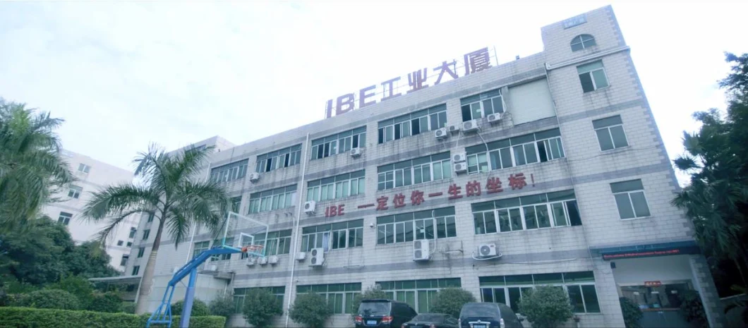
A: Our factory is located in IBE Industry Mansion,Tangtou No.1 Industry Estate,Shiyan Town,Bao’an District,Shenzhen,China, 518108
Recommended Products