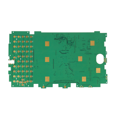
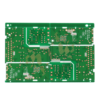
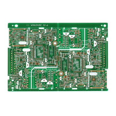
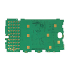
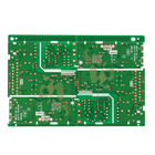
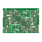
FR4 Tg150 Gold Plated 2 Layers PCB Board With V Cut Routing Inside

Contact me for free samples and coupons.
Whatsapp:0086 18588475571
Wechat: 0086 18588475571
Skype: sales10@aixton.com
If you have any concern, we provide 24-hour online help.
x| Material | FR4 Tg150 | Colour | Green,yellow,blue |
|---|---|---|---|
| Copper Thickness | 2.5oz | Acceptable Standard | IPC-A-610F Class II Or III |
| +hard Gold PlatedSurface | Gold Plated | Type | Custom Made |
| Product Name | Printed Circuit Board | Application | Industry |
| Pcb Test | Electrical Test | Min.hole Size | 0.15mm |
| Silkscreen Color | White,yellow | Layers | 2 |
| Size | 123*210mm | ||
| Highlight | FR4 Tg150 Gold Plated 2 Layers PCB,FR4 Tg150 2 layer pcb board,V Cut Routing Inside fr4 pcb board |
||
2 layers PCB gold plated with V-cut and routing inside and breakaway tab
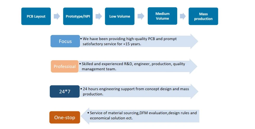
IBE Electronics Limited was established in 2005, provide one-stop services for PCB manufacturing , component sourcing, PCB assembly and testing .We have own pcb factories and SMT production lines, and a variety of professional testing equipments, company owned experienced professional and technical R & D technology team, young and professional sales and customer service teams, experienced and professional procurement team and assembly testing team, which make sure the products quality of the pass rate, on-time delivery rate of customer orders.
2 layers PCB gold plated with V-cut and routing inside and breakaway tab:
| 1 | Material | PR4,Tg150 |
| 2 | Board Thickness | 1.6mm+/-10% |
| 3 | Surface Finish | Gold plated |
| 4 | PCB Panel Size | 256*220/2 |
| 5 | Layer | 2 |
| 6 | Min. Drill Hole Size | 0.15mm |
| 7 | PCB QC | Electrical test and automatically hole inspection; Appearance automatic detection |
| 8 | Speciality | Automotive |
| 9 | Sanforized | Impedance Control |
IBE provide High quality and super service to provide quick turn and mass production on rigid PCB:
| Technical Capability of rigid PCB | ||||||||||||
| Item | Mass production | Small batch production | ||||||||||
| Number of Layers | UP TO 18L | UP TO 36L | ||||||||||
| Laminate | FR-4,Halogen free, High TG,Cem-3,Al/copper based,high frequency | |||||||||||
| Maximum board size | 610*460mm | 1200*600mm | ||||||||||
| Board thickness | 0.3-3.5mm | 0.2-6.0mm | ||||||||||
| Minimum line width/space | 3/3 mil | 3/3 mil | ||||||||||
| Minimum line/space tolerance | +/-20% | +/-10% | ||||||||||
| Max.Outer layer copper thickness | 140um | 210um | ||||||||||
| Max.Inner layer copper thickness | 105um | 175um | ||||||||||
| Min. finished hole size(Mechanical) | 0.2mm | 0.15mm | ||||||||||
| Min. finished hole size (laser hole) | 0.075mm | 0.075mm | ||||||||||
| Aspect ratio | 10:1 | 12:1 | ||||||||||
| Solder Mask Color | Green, Blue, Black,White,Yellow,Red | |||||||||||
| Impedance control Tolerance | <=+/-10% | |||||||||||
| Surface treatment | Flash Gold | 0.025-0.075um | 0.025-0.5um | |||||||||
| Immersion Gold | 0.025-0.1um | 0.1-0.2um | ||||||||||
| Sn/Pb Hasl | 1-40um | |||||||||||
| Leadfree Hasl | 1-70um | |||||||||||
| Immersion Silver | 0.08-0.3um | |||||||||||
| OSP(Entek) | 0.2-0.4um | |||||||||||
| Gold Finger(Hard Gold Plating ) | 10u''-50u'' | |||||||||||
| Other surface treatment also available such as Nickel palladium | ||||||||||||
IBE Focus on one stop solution
