


All Products
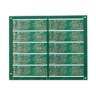
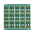
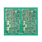
1oz Copper 2 Layers PCB Circuit Board 94V0 CCTV DVR PCB Board


| Place of Origin | Made in China |
|---|---|
| Brand Name | IBE |
| Certification | ISO 9001,ISO14001,UL |
| Model Number | IBE-9258 |
| Minimum Order Quantity | 1pc |
| Price | USD0.145 unit |
| Packaging Details | Vacuum bag+humidity indicator+carton |
| Delivery Time | 2-3 weeks |
| Payment Terms | T/T, L/C |
| Supply Ability | 100000sqm each month |

Contact me for free samples and coupons.
Whatsapp:0086 18588475571
Wechat: 0086 18588475571
Skype: sales10@aixton.com
If you have any concern, we provide 24-hour online help.
xProduct Details
| Material | FR4 Tg150 Shengyi | Colour | Black,green,yellow,blue |
|---|---|---|---|
| Copper Thickness | 1oz | Acceptable Standard | IPC-A-610F Class II Or III |
| Surface Finish | ENIG | Type | Custom Made |
| Product Name | Printed Circuit Board | Application | Bluetooth |
| Pcb Test | Electrical Test | Min.hole Size | 0.1mm |
| Silkscreen Color | White,yellow | Layers | 2 |
| Size | 57*30mm | Special | No X-out |
| Highlight | 1oz Copper 2 Layers PCB Circuit Board,94V0 CCTV DVR PCB Board,94V0 CCTV DVR 2 Layers PCB |
||
Product Description
2 layers PCB Circuit Board 94V0 CCTV DVR PCB Board Factory Supply
1/Quotes in 24 hours or less
2/Standard production leadtime of 10 working days (2-3 weeks)
3/Prototype leadtime of 2 to 5 working days (1-2 weeks)
4/Stack-ups and impedance simulation in 36 hours
5/Initial response to technical questions or quality concerns in 36 hours
6/DFM and EQ's prior to PO placement upon request
| 1 | Material | PR4,Tg150 |
| 2 | Board Thickness | 1.0mm+/-10% |
| 3 | Surface Finish | ENIG |
| 4 | PCB Panel Size | 130*190/6 |
| 5 | Layer | 2 |
| 6 | Min. Drill Hole Size | 0.1mm |
| 7 | PCB QC | Electrical test and automatically hole inspection; Appearance automatic detection |
| 8 | Application | wireless charger |
| 9 | Additional | half hole |
![]()
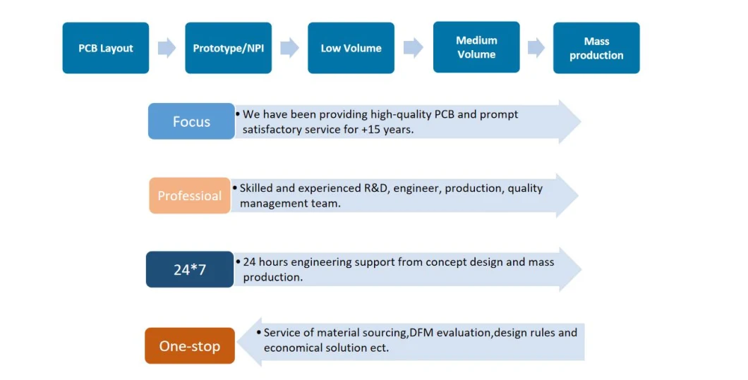
IBE provide High quality and super service to provide quick turn and mass production on rigid PCB:
| Technical Capability of rigid PCB | ||||||||||||
| Item | Mass production | Small batch production | ||||||||||
| Number of Layers | UP TO 18L | UP TO 36L | ||||||||||
| Laminate | FR-4,Halogen free, High TG,Cem-3,Al/copper based,high frequency | |||||||||||
| Maximum board size | 610*460mm | 1200*600mm | ||||||||||
| Board thickness | 0.3-3.5mm | 0.2-6.0mm | ||||||||||
| Minimum line width/space | 3/3 mil | 3/3 mil | ||||||||||
| Minimum line/space tolerance | +/-20% | +/-10% | ||||||||||
| Max.Outer layer copper thickness | 140um | 210um | ||||||||||
| Max.Inner layer copper thickness | 105um | 175um | ||||||||||
| Min. finished hole size(Mechanical) | 0.2mm | 0.15mm | ||||||||||
| Min. finished hole size (laser hole) | 0.075mm | 0.075mm | ||||||||||
| Aspect ratio | 10:1 | 12:1 | ||||||||||
| Solder Mask Color | Green, Blue, Black,White,Yellow,Red | |||||||||||
| Impedance control Tolerance | <=+/-10% | |||||||||||
| Surface treatment | Flash Gold | 0.025-0.075um | 0.025-0.5um | |||||||||
| Immersion Gold | 0.025-0.1um | 0.1-0.2um | ||||||||||
| Sn/Pb Hasl | 1-40um | |||||||||||
| Leadfree Hasl | 1-70um | |||||||||||
| Immersion Silver | 0.08-0.3um | |||||||||||
| OSP(Entek) | 0.2-0.4um | |||||||||||
| Gold Finger(Hard Gold Plating ) | 10u''-50u'' | |||||||||||
| Other surface treatment also available such as Nickel palladium | ||||||||||||
BE Focus on one stop solution
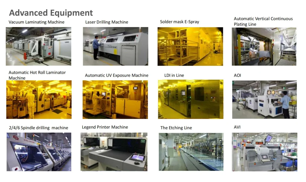
Advanced Equipment
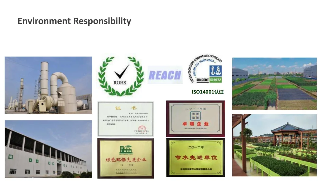
We pay attention on Environment
Recommended Products