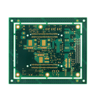
Flash Gold HDI Multilayer PCBs
IBE provides better, faster and more cost-effective solutions to our customers' most challenging design for excellence (DFx) problems. From manufacturing to testing to supply chain, IBE provides customized design support to our OEM partners, enabling them to establish a strong competitive position within their marketplace.
We have a proven record of guiding manufacturers throughout the entire electronics manufacturing process. From simple designs to complex system integration, IBE provides the end-to-end electronics manufacturing services necessary to compete in a global marketplace.
Our Advantages:
1, Factory Area:60000㎡ Shenzhen factory; two other factories in US and Vietnam.
2, Quality Control:IPC-1-610E Standard,E-test,X-ray,AOI Test,IQC,QC,QA,100% Functional Test
3, PCB Making (Rigid, Flexible,Rigid-Flexible,Aluminium, High TG,Ceramic), Component Sourcing, SMT&DIP, Free Program & Test, OEM/ODM Serivce
4, Certifcation:ATF 16949,ISO 13485,ISO 14001,ISO9001,UL(E326838),Disney FAMA, CE,FCC,ROHS,
| 1 |
Material |
PR4,Halogen free, High TG,CEM3,PTFE,Aluminum BT,Rogers |
| 2 |
Board Thickness |
Mass Production:0.3-3.5mm Samples:0.21-6.0mm |
| 3 |
Surface Finish |
HASL,OSP,Immersion Silver/Gold/SN,Flash Gold, Gold Finger,Hard Gold Plating |
| 4 |
PCB Panel Size |
Max Mass Productoin: 610x460mm Sample:762x508mm |
| 5 |
Layer |
Mass production:2-58 Layers, Samples:1-64 Layers |
| 6 |
Min. Drill Hole Size |
Laser Drill 0.1mm,Machine Drill 0.2mm |
| 7 |
PCBA QC |
X-ray,AOI Test,Functional Test |
| 8 |
Speciality |
Automotive,Medical/Gaming/Smart Device,Computer,LED/Lighting,etc |
| 9 |
Sanforized |
Buried via, Blind via, Mixed Pressure,Embedded Resistance,Embedded Capacitance, Local Mixed Pressure, Local High Density, Back Drill, Impedance Control
|
Multilayer PCB is a circuit board that has more than two layers.
Unlike a Double-Sided PCB which only has two conductive layers of material, all multilayer PCBs must have at least three layers of conductive material which are buried in the center of the material.
How Are Multilayer PCBs Made?
Alternating layers of prepeg and core materials are laminated together under high temperature and pressure to produce Multilayer PCBs. This process ensures that air isn't trapped between layers, conductors are completely encapsulated by resin, and the adhesive that holds the layers together are properly melted and cured. The range of material combinations is extensive from basic epoxy glass to exotic ceramic or Teflon materials.
Benefits of Multilayer PCBs (compared to single or double-sided PCBs)
- Higher assembly density
- Smaller size (considerable savings on space)
- Increased flexibility
- Easier incorporation controlled impedance features.
- EMI shielding through careful placement of power and ground layers.
- Reduces the need for interconnection wiring harnesses (reduces overall weight)
IBE is an Experienced Multilayer PCB Manufacturer
IBE has been producing Multilayer PCBs for over 20 years. Over the years, we have seen all types of multilayer constructions from various industries, answered all types of multilayer questions, and solved all types of problems with multilayer PCBs.