


All Products
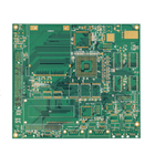
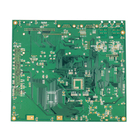
UL 2 Layer Circuit Board 9um-210um Multilayer Pcb Fabrication
| Place of Origin | China |
|---|---|
| Brand Name | IBE |
| Certification | ISO/TS16949 ISO13485 |
| Model Number | multilayer pcb |
| Minimum Order Quantity | 10 |
| Price | $0.5 |
| Packaging Details | ESD bag |
| Delivery Time | 5-8 working days |
| Payment Terms | D/A, L/C, D/A, D/P, T/T |
| Supply Ability | 50000pcs/week |

Contact me for free samples and coupons.
Whatsapp:0086 18588475571
Wechat: 0086 18588475571
Skype: sales10@aixton.com
If you have any concern, we provide 24-hour online help.
xProduct Details
| Surface Finishing | ENIG | Copper Thickness | 1oz |
|---|---|---|---|
| Base Material | FR4 | Board Thickness | 1.6mm |
| Min. Hole Size | 0.25mm | Soldermask Color | Green |
| Silkscreen Color | White | Layer | 1-32L |
| Highlight | UL 2 Layer Circuit Board,210um 2 Layer Circuit Board,210um Multilayer Pcb Fabrication |
||
Product Description
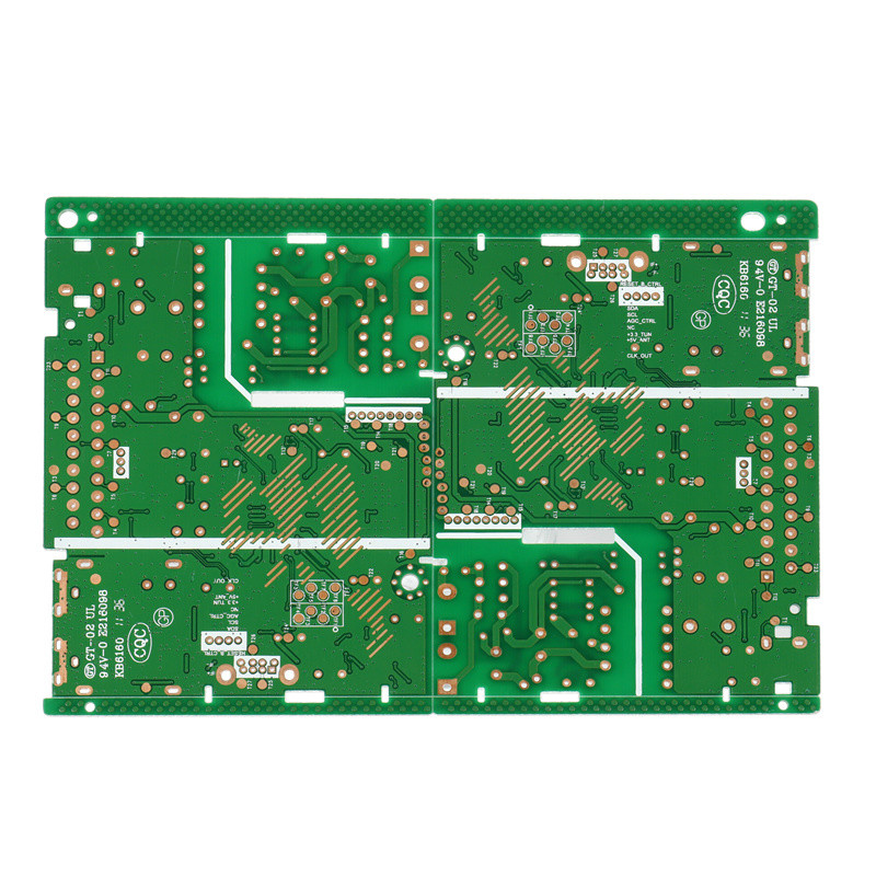
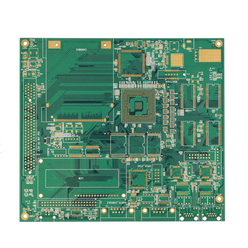
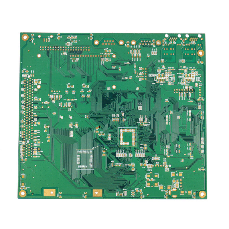
UL approval 2L&Multilayer multilayer pcb fabrication 16L RFID PCB
PCBA Capability
| PCB Manufacturing Capability | |
| PCB Layers: | 1Layers to 18 layer (Max) |
| Board thickness: | 0.13~6.0mm |
| Min line width/space: | 3mil |
| Min mechanical hole size: | 4mil |
| Copper thickness: | 9um~210um(0.25oz~6oz) |
| Max aspect ratio: | 1:10 |
| Max board size: | 400*700mm |
| Surface Finish: | HASL, immersion gold, immersion silver,immersion tin, flash gold, gold finger,peelable mask |
| Material: | FR4,High Tg, Rogers, CEM-1, CEM-3, Aluminum BT, PTFE. |
| PCB Assembly Capability | |
| Stencil size range: | 1560*450mm |
| Min SMT package: | 0402/1005(1.0x0.5mm) |
| Min IC pitch: | 0.3mm |
| Max PCB Size: | 1200*400mm |
| Min PCB thickness: | 0.35mm |
| Min Chip Size: | 01005 |
| Max BGA Size: | 74*74mm |
| BGA Ball Pitch: | 1.00~3.00mm |
| BGA Ball Diameter: | 0.4~1.0mm |
| QFP Lead Pitch: | 0.38~2.54mm |
| Testing : | ICT,AOI,X-RAY,Funtional test etc. |
Delivery Time:
|
Order Conditions
|
Standard Delivery Date
|
The fastest Delivery Date
|
|
Prototype ( <20pcs)
|
2days
|
8hours
|
|
Small Volume (20-100pcs)
|
6days
|
12hours
|
|
Medium Volume (100-1000)
|
3days
|
24hours
|
|
Mass Production (>1000)
|
Depends on BOM
|
Depends on BOM
|
FAQ:
1. What’s a motherboard?
![]()
A motherboard is a printed circuit assembly(PCA) used exclusively in laptop or desktop computers. While some may refer to a PCA as a motherboard,only those found in computers are motherboards. All other printed circuit assemblies are simply PCA or PCBA.
2.How does a printed circuit board assembly (PCB assembly) work?
![]()
The primary function of a PCB assembly is to integrate the electronic components of a device into a compact or defined space. Acting as the central hub of the electronic circuit of a device, the PCB provides insulation for all other electrical components, allowing them to be safely connected to a power source.
3. What information is required for a turnkey PCB assembly order?
For turnkey projects, we’ll need the following:
Gerber file
Bill of materials (BOM)
Component placement list (CPL)
All relevant CAD and .stp file
4. Are you UL / Underwriters Laboratory approved?
IBE pursues all applicable UL certifications for our products, and we offer several products certified with UL and CSA based on customer’s demand
Underwriters Laboratories (UL) grants multiple certifications, including:
IBE is certified for PCB by UL file E326838
5. Do you offer RoHS&REACH-compliant assemblies?
Yes, IBE does offer assemblies that comply with the European Union’s Restriction of Hazardous Substances (RoHS) Directive and REACH.
6. Do you offer testing and inspection services?
Yes, IBE offers a comprehensive list of testing and inspection services for both SMT and through-hole assemblies.
Visual inspection/scanning microscopes
AOI inspection
In-circuit test
Functional testing include automated test equipment and system
Burn-in tests
Low/High Temp Chamber Testing
X-ray inspection and repair
Salt fog tester
Drop Test
packing vibration
Conformal coating and potting
Recommended Products