


All Products
OEM 2oz Copper Multilayer PCBs 1.6mm Thickness ISO TS16949


| Place of Origin | China |
|---|---|
| Brand Name | IBE |
| Certification | ISO/TS16949 ISO13485 |
| Model Number | Electricity Meter PCBA |
| Minimum Order Quantity | 10 |
| Price | $0.1-$0.5 |
| Packaging Details | ESD bag |
| Delivery Time | 5-8 working days |
| Payment Terms | D/A, L/C, D/A, D/P, T/T, Western Union, MoneyGram |
| Supply Ability | 50000pcs/week |

Contact me for free samples and coupons.
Whatsapp:0086 18588475571
Wechat: 0086 18588475571
Skype: sales10@aixton.com
If you have any concern, we provide 24-hour online help.
xProduct Details
| Min. Line Width | 0.075mm/0.075mm(3mil/3mil) | Surface Finishing | ENIG |
|---|---|---|---|
| Copper Thickness | 1.5oz | Base Material | FR4 |
| Min. Line Spacing | 0.075mm | Board Thickness | 1.6mm |
| Min. Hole Size | 0.25mm | Soldermask Color | Green |
| Silkscreen Color | White | Layer | 1-32L |
| Highlight | OEM Multilayer PCBs 1.6mm Thickness,1.6mm Thickness 2oz Copper PCB,ISO TS16949 Multilayer PCBs |
||
Product Description
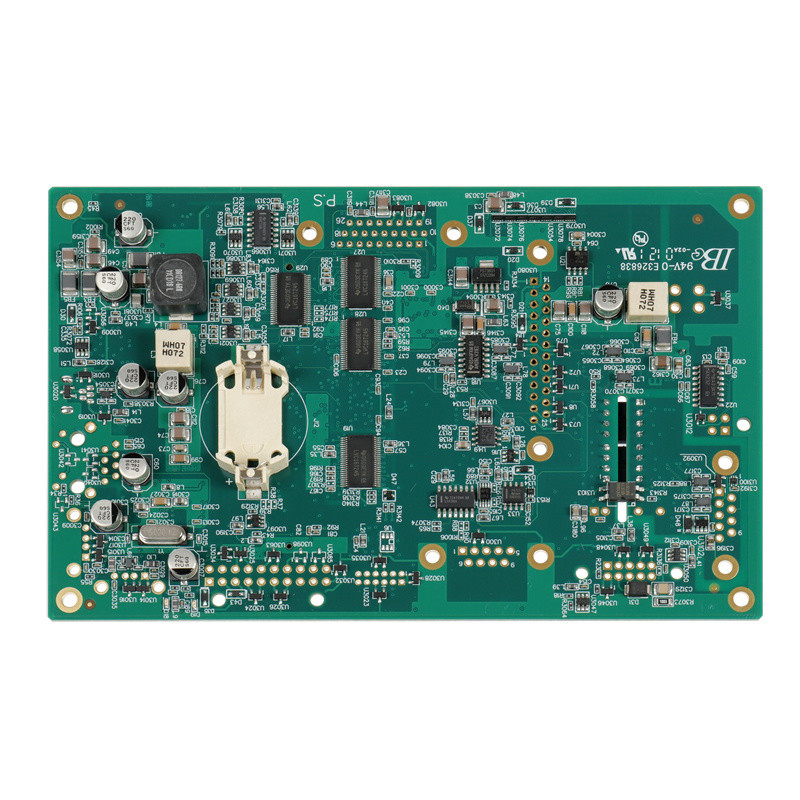
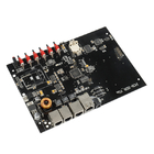
Shenzhen oem 1.6mm thickness pcb manufacturer multi layer pcba HDI Printed Circuit Board 2OZ
Advantage
1) We do PCB from double side up to 30-layer Multilayer PCB, HDI jobs.
2) If you have repeat orders from other suppliers, and you want to transfer to Intech, we can accept FREE OF TOOLING.
3) Except excellent quality and professional service, we also pay every detail for our customers, for example package to use Desiccant packs & moisture indicator in vacuum-sealed pack to protect PCB.
4) Material: We have FR4 TG135/TG158/TG180 normal material in stock, also have FR1/ FR2/ FR3/ CEM1/ CEM3/ ROGERS/ ARLON/ ISOLA.
5) Rigid / flex/ flex-rigid PCBs with UL approved.
6) Flexible,quickly feedback for customers always.
![]()
| PCB Manufacturing Capability | |
| PCB Layers: | 1Layers to 18 layer (Max) |
| Board thickness: | 0.13~6.0mm |
| Min line width/space: | 3mil |
| Min mechanical hole size: | 4mil |
| Copper thickness: | 9um~210um(0.25oz~6oz) |
| Max aspect ratio: | 1:10 |
| Max board size: | 400*700mm |
| Surface Finish: | HASL, immersion gold, immersion silver,immersion tin, flash gold, gold finger,peelable mask |
| Material: | FR4,High Tg, Rogers, CEM-1, CEM-3, Aluminum BT, PTFE. |
| PCB Assembly Capability | |
| Stencil size range: | 1560*450mm |
| Min SMT package: | 0402/1005(1.0x0.5mm) |
| Min IC pitch: | 0.3mm |
| Max PCB Size: | 1200*400mm |
| Min PCB thickness: | 0.35mm |
| Min Chip Size: | 01005 |
| Max BGA Size: | 74*74mm |
| BGA Ball Pitch: | 1.00~3.00mm |
| BGA Ball Diameter: | 0.4~1.0mm |
| QFP Lead Pitch: | 0.38~2.54mm |
| Testing : | ICT,AOI,X-RAY,Funtional test etc. |
Delivery Time:
|
Order Conditions
|
Standard Delivery Date
|
The fastest Delivery Date
|
|
Prototype ( <20pcs)
|
2days
|
8hours
|
|
Small Volume (20-100pcs)
|
6days
|
12hours
|
|
Medium Volume (100-1000)
|
3days
|
24hours
|
|
Mass Production (>1000)
|
Depends on BOM
|
Depends on BOM
|
FAQ:
1.How does a printed circuit board assembly (PCB assembly) work?
![]()
The primary function of a PCB assembly is to integrate the electronic components of a device into a compact or defined space. Acting as the central hub of the electronic circuit of a device, the PCB provides insulation for all other electrical components, allowing them to be safely connected to a power source.
2. What information is required for a turnkey PCB assembly order?
For turnkey projects, we’ll need the following:
Gerber file
Bill of materials (BOM)
Component placement list (CPL)
All relevant CAD and .stp file
3. Are you UL / Underwriters Laboratory approved?
IBE pursues all applicable UL certifications for our products, and we offer several products certified with UL and CSA based on customer’s demand
Underwriters Laboratories (UL) grants multiple certifications, including:
IBE is certified for PCB by UL file E326838
Recommended Products