


All Products
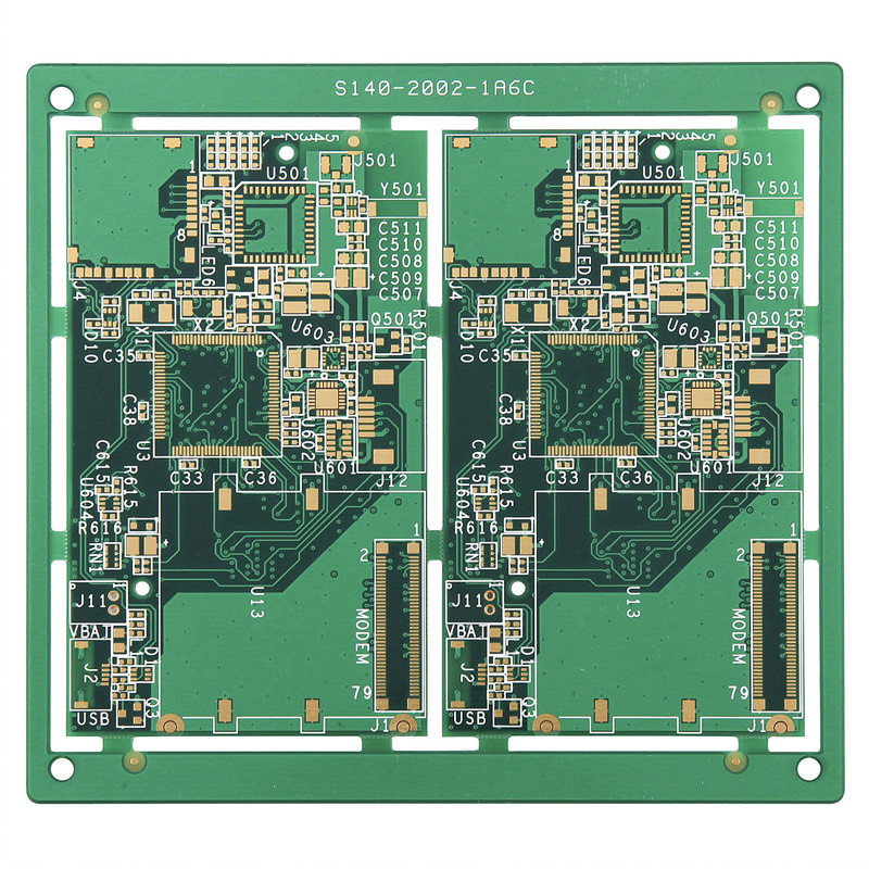
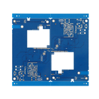
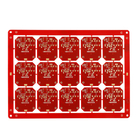
1oz Multilayer Pcb Fabrication 12 Layer Circuit Board ISO TS16949


| Place of Origin | China |
|---|---|
| Brand Name | IBE |
| Certification | ISO/TS16949 ISO13485 |
| Model Number | multilayer pcb |
| Minimum Order Quantity | 10 |
| Price | $0.1-$0.5 |
| Packaging Details | Vacuum Package |
| Delivery Time | 5-8 working days |
| Payment Terms | D/A, L/C, D/A, D/P, T/T, Western Union, MoneyGram |
| Supply Ability | 50000pcs/week |

Contact me for free samples and coupons.
Whatsapp:0086 18588475571
Wechat: 0086 18588475571
Skype: sales10@aixton.com
If you have any concern, we provide 24-hour online help.
xProduct Details
| Min. Line Width | 0.075mm/0.075mm(3mil/3mil) | Surface Finishing | ENIG |
|---|---|---|---|
| Copper Thickness | 1oz | Base Material | FR4 |
| Min. Line Spacing | 0.075mm | Board Thickness | 1.6mm |
| Min. Hole Size | 0.25mm | Soldermask Color | Green |
| Silkscreen Color | White | Layer | 1-32L |
| Highlight | 1oz Multilayer Pcb Fabrication,12 Layer Circuit Board ISO TS16949,1oz 12 Layer Circuit Board |
||
Product Description
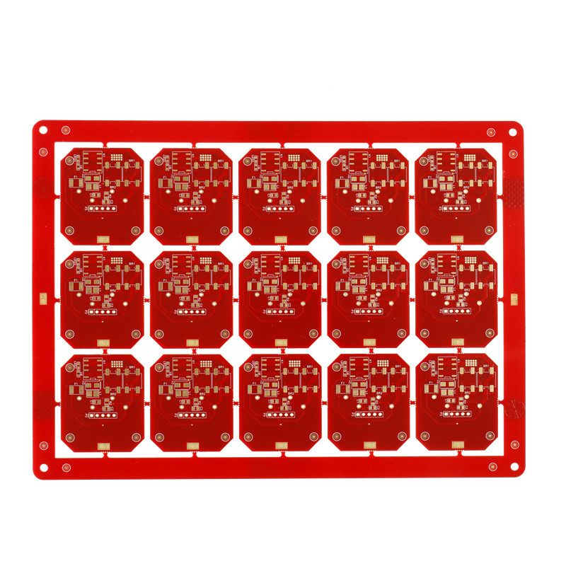
One-Stop fr4 high tg multilayer pcb fabrication 12layers pcb
![]()
| PCB Manufacturing Capability | |
| PCB Layers: | 1Layers to 18 layer (Max) |
| Board thickness: | 0.13~6.0mm |
| Min line width/space: | 3mil |
| Min mechanical hole size: | 4mil |
| Copper thickness: | 9um~210um(0.25oz~6oz) |
| Max aspect ratio: | 1:10 |
| Max board size: | 400*700mm |
| Surface Finish: | HASL, immersion gold, immersion silver,immersion tin, flash gold, gold finger,peelable mask |
| Material: | FR4,High Tg, Rogers, CEM-1, CEM-3, Aluminum BT, PTFE. |
| PCB Assembly Capability | |
| Stencil size range: | 1560*450mm |
| Min SMT package: | 0402/1005(1.0x0.5mm) |
| Min IC pitch: | 0.3mm |
| Max PCB Size: | 1200*400mm |
| Min PCB thickness: | 0.35mm |
| Min Chip Size: | 01005 |
| Max BGA Size: | 74*74mm |
| BGA Ball Pitch: | 1.00~3.00mm |
| BGA Ball Diameter: | 0.4~1.0mm |
| QFP Lead Pitch: | 0.38~2.54mm |
| Testing : | ICT,AOI,X-RAY,Funtional test etc. |
Delivery Time:
|
Order Conditions
|
Standard Delivery Date
|
The fastest Delivery Date
|
|
Prototype ( <20pcs)
|
2days
|
8hours
|
|
Small Volume (20-100pcs)
|
6days
|
12hours
|
|
Medium Volume (100-1000)
|
3days
|
24hours
|
|
Mass Production (>1000)
|
Depends on BOM
|
Depends on BOM
|
FAQ:
1.How does a printed circuit board assembly (PCB assembly) work?
![]()
The primary function of a PCB assembly is to integrate the electronic components of a device into a compact or defined space. Acting as the central hub of the electronic circuit of a device, the PCB provides insulation for all other electrical components, allowing them to be safely connected to a power source.
2. What information is required for a turnkey PCB assembly order?
For turnkey projects, we’ll need the following:
Gerber file
Bill of materials (BOM)
Component placement list (CPL)
All relevant CAD and .stp file
3. Do you offer testing and inspection services?
Yes, IBE offers a comprehensive list of testing and inspection services for both SMT and through-hole assemblies.
Visual inspection/scanning microscopes
AOI inspection
In-circuit test
Functional testing include automated test equipment and system
Burn-in tests
Low/High Temp Chamber Testing
X-ray inspection and repair
Salt fog tester
Drop Test
packing vibration
Conformal coating and potting
4.Where do you manufacture your products?
We have production plant based in shenzhen,China; Fremont,US,Bac Ninh,Vietn
Recommended Products